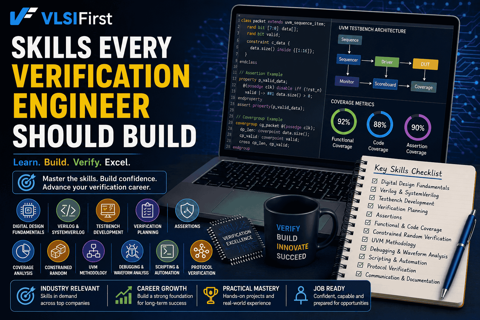
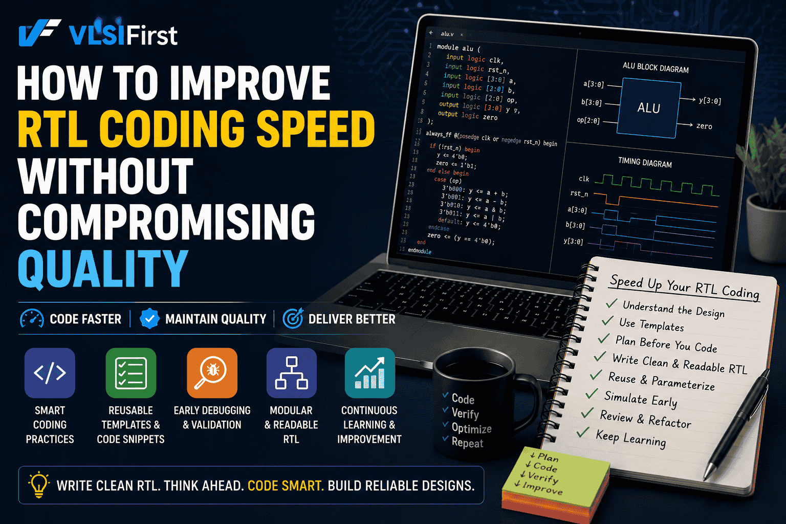
The demand for VLSI Verification Engineers continues to surge with the growth of AI chips, 5G, autonomous vehicles, and edge computing. If you're a beginner from electronics, ECE, or electrical background, entering this domain might seem overwhelming. But with a structured roadmap, even a fresher can transition from “zero” to “job-ready” in less than a year—or faster with smart effort.
This blog outlines a step-by-step roadmap designed for beginners to master VLSI Verification, based on what top Indian and global semiconductor companies are expecting today.
Phase 1: Build Your Fundamentals (Week 1–3)
Even before touching UVM or SystemVerilog, you need to lay a solid foundation in digital electronics and hardware design.
Key Topics to Cover:
Number Systems, Boolean Algebra
Combinational and Sequential Circuits
FSM (Finite State Machines)
Timing Diagrams and Flip-Flop operations
RTL vs. Gate-level vs. Transistor-level design
Synchronous vs Asynchronous design
Recommended Free Resources:
NPTEL Digital Design by Prof. Janakiraman
All About Circuits – Digital section
YouTube: VLSIFirst
Paid Options:
Basic VLSI Design courses on Udemy/Coursera (₹500–₹2000)
VLSI verification foundation programs by VLSIFirst training institute
Phase 2: Learn HDL – Verilog (Week 4–6)
You cannot do verification without knowing how the design is written. Verilog HDL is still the most preferred RTL language in the Indian job market.
Topics to Focus:
Verilog Data types, operators
Behavioral vs Structural modeling
Testbench writing basics
Blocking vs Non-blocking statements
Simulation Flow
Tools to Use:
Free: Icarus Verilog + GTKWave
Paid: ModelSim, available with many student training kits
Tip:
Try writing small modules—like ALU, counter, shift registers—and simulate them. Build confidence before diving into testbench creation.
Phase 3: Enter the World of Verification (Week 7–10)
Here comes the heart of your roadmap—understanding how to test chips before tape-out.
Learn These Core Concepts:
Testbenches and simulation flows
Directed Testing vs Constrained Random Testing
Assertion-Based Verification (ABV)
Functional coverage
Role of simulators like VCS/Questa
Suggested Free Playgrounds:
EDA Playground (edaplayground.com) – Practice Verilog, SV, UVM online
TL-Verilog with Makerchip (great for visual learners)
Phase 4: Master SystemVerilog (Week 11–15)
Now that you're clear with Verilog and verification flow, it's time to step up to SystemVerilog—the universal standard for modern verification.
Focus Areas:
SystemVerilog Data Types
Interfaces, Classes, Inheritance
Randomization & Constraints
Functional Coverage
Assertions
Building Transaction-Level Models
Practice Ideas:
Create a SystemVerilog testbench for a FIFO or UART design
Add coverage and assertions to evaluate correctness
Resources:
Free: AMIQ Blog, SystemVerilog tutorials on YouTube
Paid: VLSI verification courses with hands-on SV/UVM
Phase 5: Get Comfortable with UVM (Week 16–20)
Most job roles in VLSI verification today demand working knowledge of the Universal Verification Methodology (UVM).
What to Learn:
UVM Architecture: Components, Phases
Sequence, Driver, Monitor, Scoreboard
Factory and Configuration
Reporting and TLM communication
Environment construction and hierarchy
Projects to Try:
Build a UVM environment for a basic protocol (UART/SPI)
Add functional coverage and constrained random stimulus
Debug using waveform analysis
Tools:
Synopsys VCS
QuestaSim Student Edition
Xilinx Vivado for interfacing design + testbench (free WebPack)
Phase 6: Mini Projects & Real-World Practice (Week 21–24)
This is where you prove your skills. Mini-projects help you link everything you’ve learned and prepare for real interviews.
Mini Project Ideas:
UVM testbench for AXI-lite or AHB protocol
Constrained random verification for a FIFO or arbiter
Verification IP for UART with coverage metrics
Where to Find Open Projects:
GitHub repositories (search "UVM Projects")
VLSIIndia forums & training partners’ alumni portals
Public IP cores (like OpenCores.org)
Phase 7: Resume, Mock Interviews & Job Applications (Week 25–30)
Once your skills are built, it's time to enter the job race with confidence.
Build a Strong Resume:
Mention tools: Verilog, SystemVerilog, UVM, ModelSim, VCS
Highlight projects, especially self-built UVM environments
Add GitHub/LinkedIn links for visibility
Practice Mock Interviews:
Many online training providers offer 1:1 interview support
YouTube: Mock VLSI verification interviews
Platforms like AmbitionBox and LinkedIn Learning offer scenario-based quizzes
Top Hiring Roles in 2026:
VLSI Verification Intern (for 3rd/4th-year students)
Junior Verification Engineer
RTL + Verification Engineer (hybrid)
IP Verification Engineer
Keep Learning Protocols – AMBA, AXI, AHB, PCIe are hot in verification Subscribe to Semiconductor Journals/Blogs Join LinkedIn Groups like “VLSI Career Guide 2025” or “VLSI Fresher Jobs India” Attend VLSI Webinars (Synopsys, Cadence, DVCon India) You don't need a Master’s degree or expensive certification to crack a VLSI verification job. What you need is: Consistency Clear roadmap Hands-on practice Passion for debugging and quality This roadmap gives you a structured 30-week journey from scratch to job-ready, and with dedication, you can shorten that timeline even further. The semiconductor industry is waiting for skilled verification engineers. Are you ready to be one of them?Tips to Stay Ahead
Final Words