

Physical Design
Acquire industry relevant skills in Physical Design and gain hands-on
project experience with tools like ICC and Fusion-Compiler, ensuring
you are job-ready in the thriving semiconductor field.

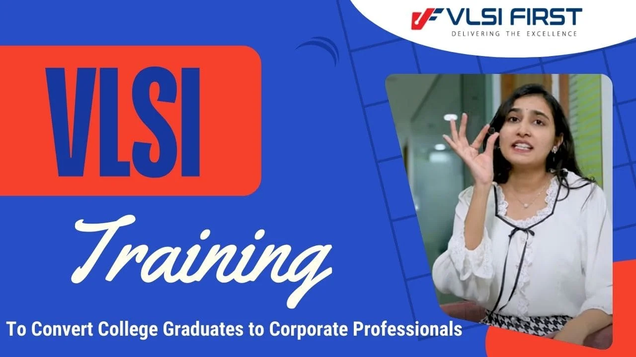
Our Physical Design Course offers a comprehensive understanding of VLSI design flows, focusing on synthesis and optimization to achieve improved power, performance, and area (PPA). You’ll gain in-depth knowledge of static timing analysis (STA) from synthesis through to physical design signoff, as well as the complete physical design process from floorplanning to post-route. The course includes practical exposure to industry tools, along with valuable experience in real-world challenges through demo projects. You'll also learn scripting with Shell and TCL to enhance efficiency. With access to online study materials and library facilities, you’ll receive placement assistance and mock interview preparation under the guidance of industry experts, ensuring you are well-equipped for success in the semiconductor industry.
- Evolution of VLSI
- VLSI Design flow cycle
- Semiconductor Eco-system
- What is ASIC & FPGA
- FPGA design flow & ASIC design and verification flow
- SoC architecture
- SoC Design flow
- Opportunities for VLSI engineers in India
- VLSI industry work profiles and roles
- How to be industry ready?
- Number system introduction & radix conversion
- Complements of number systems
- Basics/complex gates operation & truth table
- NAND & NOR realization
- Boolean function implementation & optimization
- Multiplexer realization
- Introduction to sequential circuits (flip-flops & latches)
- Master–slave combination & its limitations
- Edge/level triggering & its advantages/disadvantages
- Synchronous & asynchronous circuits
- Frequency divider circuit
- Basics of N-Type & P-Type semiconductor.
- PN Junction Operation.
- Basics of MOSFET (PMOS/NMOS) ,CMOS & FinFet.
- Realization of Gates using MOSFET.
- Understanding of basics CMOS operation.
- CMOS Short Channel Effect , CMOS Leakage Current, DIBL effect.
- MOSFET Power consumption & Drain Current equation.
- Transistor Skewing & its effect.
- CMOS Fabrication Steps.
- Realization of D-Flip Flop using Transmission Gate.
- Linux Commands
- How to work with Gvim Editor Tool
- Shortcuts & Tricks
- Introduction - Why verilog, Language Concepts, and abstraction levels
- What is DUT and TB How to use Questa Sim and see the waveform and netlist
- Verilog Module and Dataflow Modelling
- DataTypes - whitespaces, comments, Strings, Numbers, Net, Reg, Vectors, Integer, Real, Time, Arrays
- Operators (Intro and Concatenation, Shift, Relational, Equality, Conditional, Arithmatic)
- Operators (Logical, Bitwise, Reduction)
- System Tasks and Compiler directives
- Gate Level Modeling (ALL gates and one circuit)
- Switch level (NAND)
- Structural Modeling (FA and MUX and mux from decoder and tristate buffers)
- Behavioural Modeling - Blocking vs Non-Blocking, if-else and Case and Loops
- Behavioural Modeling - All Flipflops
- Behavioural Modeling - Registers
- Behavioural Modeling - Counters, FSM Design
- What is Physical Design ?
- Physical Design Flow
- Inputs required for Physical Design
- Introduction to STA
- STA Flow & Integration
- STA Concepts & Terminologies
- Timing Parameters
- Slack Calculations
- Clock Skew
- Constraints in STA
- Design Rule Violations (DRV)
- Timing Reports
- Timing Arcs & Types
- Understanding Industrial Design Flow
- Inputs of Synthesis
- Logical aware & Physical aware Synthesis
- Synthesis Flow
- Synthesis optimization Techniques
- Advantages & Disadvantages of Synthesis
- Outputs of Synthesis
- Introduction to Sanity Checks
- Types Of Sanity Checks
- Introduction to Floor Plan
- Inputs of Floor Planning
- Creating Core & Die
- Shape & Size of the Block (Aspect Ratio)
- Macro Placement & Guidelines
- Ports & Pads Placement
- Blockages & Types
- Physical only cells placement
- Checks & Outputs
- Introduction to Power Planning
- Types of Power Consumptions
- PDN
- IR Drop Analysis & Fixes
- Electro Migration Causes & Fixes
- Methods of Power Planning
- Contents in UPF
- Power Optimization Techniques
- Checks & Outputs of Power Plan
- Introduction to Placement
- Inputs of Placement
- Timing driven & Congestion driven Placement
- Stages in Placement
- Reason for Congestion & Fixes
- Reason for Timing Failure & Fixes
- Fixes for DRV's
- Bounds & Types
- Path grouping
- Magnet Placement
- Checks & Outputs of Placement
- Introduction to CTS
- Inputs of CTS
- CTS Flow
- CTS Exceptions & Clock Tree Methodology
- Latency & Skew optimization
- CTS optimization Techniques
- NDR's
- Clock Routing Methodology
- Checks & Outputs of CTS
- Introduction to Routing
- Inputs of Routing
- Routing Flow
- Routing optimization Techniques
- Stages of Routing
- Routing Switches
- Routing Algorithms
- Checks & Outputs of Routing
- Introduction to Sign-Off
- Signal Integrity & Cross Talk Analysis
- Fixes of Cross Talk
- Antenna Violation & Fixes
- ECO Flows
- Introduction to Physical Verification
- LVS Checks
- ERC
- DRC
- DFM
- Low Power Checks
- Goals & Outputs of Physical Verification
- Timing Exceptions
- Uncertainity
- MMMC Analysis
- External Timing Concepts
- Special Timing Paths
- PBA & GBA Analysis
- Slack Calculations with uncertainity
- Derates
- Unateness
- Introduction to TCL
- TCL operators
- TCL control statements (if-else, while, for, foreach)
- TCL strings & their applications
- TCL lists
- TCL arrays
- TCL file handling operations
- TCL regular expressions
- TCL procedures
- TCL program examples & practice session
Trainees will work on industry-standard RTL-to-GDSII projects focused on optimizing for minimum area, low power, and high performance. Each project simulates real-world block-level physical design, requiring candidates to deliver a clean, sign-off-ready GDSII from the given input database.
- Creating a Unique Resume: Learn strategies to design a resume that reflects your individuality and aligns with industry expectations.
- Highlighting Technical Skills: Identify and list the most relevant technical skills that add value to your profile.
- Project Descriptions & Roles: Master the art of describing your projects, roles, and responsibilities effectively to demonstrate real-world experience and measurable impact.
- Mock Interviews & Practice Sessions: Participate in simulated interviews that mirror real industry scenarios.
- Interview Practice with Industry Experts: Gain insights and guidance directly from professionals working in your target domain.
- Personalized Feedback: Receive constructive feedback on your performance to help you improve and excel in future interviews.


off








Affordable fee
Structure
Student can pay in No cost EMI for 5 months.
Students are Eligible for Internship.
As per hiring companies requirement, as our trainers are working in industry they update course content time to time
OTHER INSTITUTE
High Fee.
No Fee after placement option
They ask to clear total fee within 1 month.
No scholarships provided.
Why VLSIfirst is Highest Rated?
About Placement
We are a leading provider of VLSI training solutions, dedicated to empowering engineers with the skills and knowledge required to excel in the semiconductor industry.
Our Approach:
- Integrated Training: Blend of theory and practical application.
- Real-World Preparation: Equipping students for practical challenges
- Comprehensive Approach: Holistic training for robust skill development.


Our work with clients has always been at the intersection of deep industry expertise and extensive capabilities.
Fee Structure:
Total fee: 1,00,000/ Student need to pay 75,000 in Training Period
15000/- for Registration
15000/- after 1 st Month
15000/- after 2 nd Month
15000/- after 3 rd Month
15000/- after 4 th Month
Remaining 25,000 after getting placement (after receiving offer letter from company)
No, if you get placement through your sources there is no need to pay 25% fee, however, you need to inform us that you want to try on your own as soon once you finish your training.
No, you will pay 25% fee after placement only.
No, we don’t offer any discounts in fee.
We provide offline classes in 3 locations, Hyderabad, Bangalore and Noida
Yes, any student who are passedout between 2005 to 2024 can join the course
Didn't find what you were looking for?
Contact UsBooking Appointment
Speak With Industry Experts
Enroll in our comprehensive Physical Design Course in India designed to equip you with the essential skills and knowledge required in the field of physical design. This course covers all fundamental concepts, including floor planning, place and route, and design rule checks, preparing you for real-world applications. With expert instructors leading the way, you'll receive hands-on training and valuable insights into the latest tools and techniques used in the industry.
Physical Design Certification and Institute in India
Upon completing our Physical Design Certification Course in India, you will gain a recognized credential that enhances your employability in the competitive job market. Our Physical Design Institute in India is committed to providing high-quality education, ensuring that you are well-prepared for a successful career. Our certification is respected by leading employers, giving you an edge in securing job opportunities in physical design
Job-Oriented Physical Design Training in India
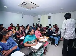
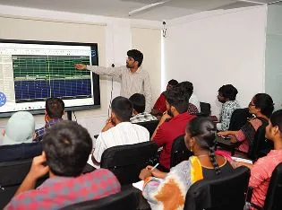
Join our Physical Design Class at our esteemed Physical Design Training Institute in India, where we offer a Physical Design Job-oriented course designed to prepare you for success in the industry. Our curriculum emphasizes practical skills and real-world applications, ensuring you gain the expertise needed for today's job market. As part of the program, you'll have the opportunity to participate in a Physical Design Internship in India, providing you with valuable hands-on experience and a competitive edge when applying for jobs. Enroll today to take the first step toward a rewarding career in physical design!
Our Physical Design Online Training in India is tailored for those looking to balance learning with their professional commitments. We also offer a Placement Assured Physical Design Training program in India, which includes an internship opportunity to give you hands-on experience. Join our Physical Design Bootcamp in India for an intensive learning experience, ensuring you're job-ready and equipped to thrive in a dynamic industry.
Hours
Copyright 2025 © VLSI Technologies Private Limited
Designed and developed by KandraDigitalCopyright 2025 © VLSI Technologies Private Limited
Designed, Developed & Marketing by KandraDigital