

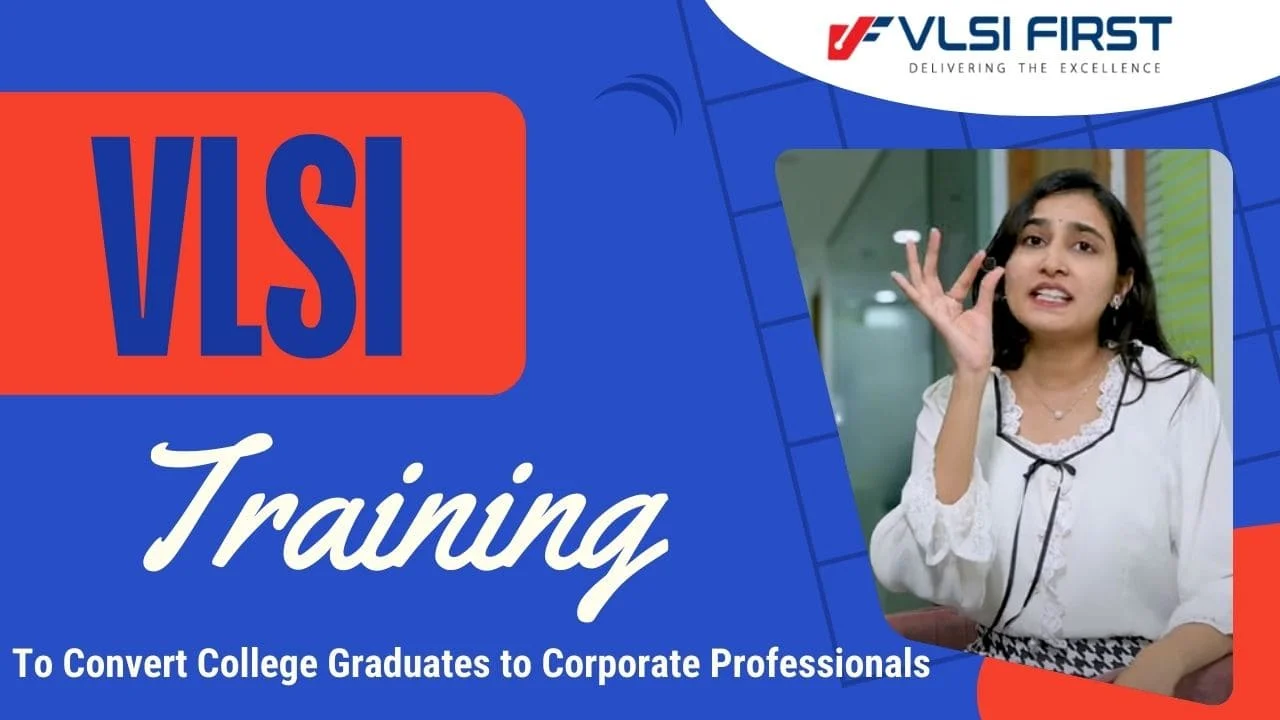
Design and Verification in pune

VLSI (Very Large Scale Integration) RTL (Register Transfer Level) Design and Verification is the process of designing and verifying the functionality of the digital circuits. This process involves implementing circuits using hardware description languages (HDLs) like Verilog or VHDL. RTL Design involves creating a high-level behavioral description of the digital circuit that specifies its functionality, and then translating this description into a register transfer level (RTL) description. The RTL description is a low-level representation of the circuit that specifies the behavior of each individual gate and the connections between them. The RTL description is then used to synthesize the circuit into a gate-level netlist, which can be used to implement the design in hardware.
- Evolution of VLSI
- VLSI Design flow cycle
- Semiconductor Eco-system
- What is ASIC & FPGA
- FPGA design flow & ASIC design and verification flow
- SoC architecture
- SoC Design flow
- Opportunities for VLSI engineers in India
- VLSI industry work profiles and roles
- How to be industry ready?
- Number Systems and conversions
- Number System complements (Binary Arithematics - Addition and Subtraction)
- Boolean algebra, Boolean theorems and laws, Sum of products and product of sums, Minterms and Maxterms
- Karnaugh map Minimization
- Logic gates, Enable & disable concept of gates, Tristate logic gates
- Binary Codes – Binary, BCD, Excess 3, Gray
- Error detection & correction - Parity method
- Hazards in combinational circuits
- Half Adder, Full Adder, RCA
- Multiplexer, Demultiplexer
- Encoders, Priority Encoders
- Decoder (Active high & low outputs), Magnitude Comparator
- Sequential circuits: Latches (SR Latch, S'R' latch), gated latch (SR, D latch)
- Clock - Triggering types, clock duty cycle, clock jitter, glitches & skew
- Sequential circuits: Flipflops & types (characteristic and excitation tables)
- Master/Slave FF – Operation, timing diagrams
- Shift registers - SISO, SIPO, PISO, PIPO
- Shift registers - Universal Shift Register, Bidirectional
- Design of Counters- Asynchronous Counters - Up, Down, Up-Down counters, Ring Counter, Jhonson counter
- Synchronous Counters - Up, Down, Up-Down counters
- Clock generation, Setup time, Hold time, Metastability and frequency calculations, frequency division using counters
- State Machines Design – Moore models (Overlapping & Non Overlapping)
- Mealy models (Overlapping & Non Overlapping)
- Memory structure - ROM/ RAM
- Synchronous FIFO
- Asynchronous FIFO
- Linux Commands
- How to work with Gvim Editor Tool
- Shortcuts & Tricks
- Introduction to HDL
- Differences b/w high level language (C Programming) and HDL, VHDL vs Verilog HDL, VLSI Design Flow cycle.
- Introducing RTL Design (DUT) and Testbench
- Defining RTL Design (DUT) and Verilog Testbench, Structure of DUT and Verilog Testbench.
- What are Ports and types?
- What is Instantiation?
- Compilation vs Simulation vs Synthesis
- Modelling Styles-Levels of Abstraction
- Data Flow Modelling- Implicit Continuous Assignments
- Tool Introduction with basic gates or MUX example in Dataflow modelling along with TB
- Basic Concepts- Lexical Conventions (White Spaces, Comments, Operators, Number Specifications, Strings, Keywords, Identifiers)
- Data Types (Net Data Types, Register Data Types), System Tasks, Defines, Parameters, timescale
- Operators (Concatenation, Replication, Negation, Unary Reduction, Arithmetic, Shift, Relational, Equality Logical, Case, Bit-wise, Logical-wise, Conditional)
- Modelling Styles- Gate Level Modelling- Gate Level Primitives (and, or, nand, nor, xor, xnor, not)
- Structural Modelling-Instantiation- Naming, Positioning, Example-Ripple Carry Adder
- Behavioural Modelling- Procedural Blocks- initial and always, Sensitivity list, Blocking assignments/statements
- Behavioural Modelling- Non-blocking assignments/statements, Inter and Intra Delays
- Verilog Stratified Queues (Verilog Regions)- Active, Inactive, NBA, Monitor/Postponed Regions
- Behavioural Modelling- If-else (2x1 and 4x1 Mux), case, casex, casez (4x1 Mux, Priority Encoder)
- Behavioural Modelling- Looping Statements- for, repeat, while, forever, begin-end, fork-join, naming of blocks, disable
- Verilog Functions- Introduction, formal arguments, actual arguments, function call, example- Ripple Carry Adder
- Verilog Tasks- Introduction, example- Ripple Carry Adder, Task based Testbench
- Verilog Coding- Arrays, Memories (ROM)
- Verilog Coding- Memories (RAM)
- Verilog Coding- Finite State Machines (Moore, Mealy -- Overlap, Non-overlap)
- Verilog Coding- Synchronous FIFO
- Modelling Styles- Switch Level Modelling- PMOS, NMOS, CMOS- NOT, NAND, NOR, AND, OR Gates (optional)
- Testbench approaches - Self checking testbench, Linear TB, Random TB
- Compiler Directives ('ifdef, 'ifndef, 'endif, 'else)
- $value$plusargs, Force-Release, ceil, log
- Clock generation and frequency calculations, frequency division using counters, clock duty cycle
- File Handling's in verilog, PLI (optional)
- Generate block - Genvar Keyword, Specify block and UDP (optional)
- Importance of Verification
- Difference b/w Design & Verification
- Difference b/w HDL & HVL
- Challenges in Verification
- Verification Flow
- Roles & Types in Verification
- Difference Verilog & System Verilog
- Why System Verilog prefered over verilog
- Functional Verification vs Formal Verification
- Introduction of System Verilog
- Necessity to migrate from Verilog --> SV --> UVM
- Architecture of SV Environment
- Data types - Enum, Typedef, Structure, Union, Class
- Arrays - Fixed Array (Packed and Unpacked), Dynamic Array, Associative Array, Queues
- Array methods - ordering, reduction, locator, index querying methods
- loops - Enhanced for loop, foreach, while, dowhile, repeat,forever
- Procedural Statements and Flow Control - Conditional statements (unique if, priority if, unique case, priority case)
- jump statements
- statement labels
- disable statements
- new procedural blocks (always_comb,always_latch,always_ff,final)
- Process control - fork_join, fork_join_any, fork_join_none, wait fork and disable fork
- Class - Nested/Aggregated class
- SV subroutines - Function & Task, Argument types and Argument Passing Types, Static and Automatic Methods
- Randomization - Why Randomization?, rand and randc keywords , Randomization methods, Randomization of scope variables, How to disable Randomization, How we can control Randomization
- Constraints - Inline, inside, unique, soft, Implication, weighted, static and iterative, function inside constraint, bi-directional and solve before
- Shallow copy & Deep Copy
- Interprocess communication - Semaphore, Mailbox, Events and wait_order
- OOPS - Inheritance, Constraint Inheritance, Casting (static & Dynamic), Data hiding and Encapsulation, Abstract Class, Polymorphism, Pure Virtual Methods, Parameterized class & typedef class
- Interface -Modports, Clocking Block, Program Block
- SV regions
- SV Environment with all the components
- Introduction to Coverage Driven Constraint Random Verification (CDCRV)
- Types of Coverages (Code & Functional)
- Brief about Functional Coverages
- Coverage Bins (Implicit & Explicit)
- Different types of bins (Transition, Binsoff, intercept)
- Conditional Coverage
- coverage options
- Introduction to Assertion Based Verification (ABV)
- Need and Types of Assertions
- Immediate Assertion"
- SVA Building Blocks
- Introduction to Concurrent Assertions
- Assertions Built-in methods
- SVA Binding
- User defined macros
- SV Packages
- Introducing DPI
- Verification Plan Document or V Plan
- Verification Architecture
- Feature Extraction and creating Test plan
- Coverage Plan
- Assertion Plan
- FIFO SV-TB Development
Introduction to Methodology
- What is UVM?
- Why UVM?
- Overview of UVM Structure.
UVM Testbench Architecture
- Test Bench Structure
- Explanation of Test Bench
- UVM Objects and UVM Components
- UVM Sequence Item
- UVM Sequence and UVM Sequencer
- UVM Driver and UVM Monitor
- UVM Agent and UVM Scoreboard
- UVM Test and UVM Top.
UVM Phases
- Types of Phases
- Explanation of Phases
UVM TLM
- Analysis Port
- Usage of TLM Ports
- Declaration and Connection of Ports
UVM Reporting
- Reporting Methods
- Configurations
- Usecases
UVM Configurations
- Usage of Configurations
- Set Config Methods
UVM Factory
- Registration
- Factory Methods Explanation
UVM Callback
- Body Call back
- Usage and Importance of Call Backs
Sequences
- Overview and Implementation of Sequences.
UVM Macros
- Macros Explanation in UVM.
UVM Project
- UVC Development for Industry standard protocol.
- Explanation of IP, VIP, SOC Level Testbench flow, Testplans, Verification plan.
Register Layer
- Introduction
- Register Model
- Register Environment
- Connection of Register Environment
Lock Grab
- Examples
- Arbitration
- Importance of Arbitration
- Usage of Arbitration
- Sequencer Arbitration
- Virtual Sequence, Sequencer
- Need and Usage of Virtual Sequence and Sequencer.
- Understanding APB Protocol
- Developing UVM environment for APB
- Developing Test cases
- RTL Design Project based on Verilog
- Verification Project based on UVM
All the projects delivered are as per industry standard implementations of High speed protocols/Memories/RISC-V/Interconnects
- Creating a Unique Resume: Learn strategies to design a resume that reflects your individuality and aligns with industry expectations.
- Highlighting Technical Skills: Identify and list the most relevant technical skills that add value to your profile.
- Project Descriptions & Roles: Master the art of describing your projects, roles, and responsibilities effectively to demonstrate real-world experience and measurable impact.
- Mock Interviews & Practice Sessions: Participate in simulated interviews that mirror real industry scenarios.
- Interview Practice with Industry Experts: Gain insights and guidance directly from professionals working in your target domain.
- Personalized Feedback: Receive constructive feedback on your performance to help you improve and excel in future interviews.


off


Affordable fee
Structure
Student can pay in No cost EMI for 5 months.
Students are Eligible for Internship.
As per hiring companies requirement, as our trainers are working in industry they update course content time to time
OTHER INSTITUTE
High Fee.
No Fee after placement option
They ask to clear total fee within 1 month.
No scholarships provided.
Why VLSIfirst is Highest Rated?

About Placement
We are a leading provider of VLSI training solutions, dedicated to empowering engineers with the skills and knowledge required to excel in the semiconductor industry.
Our Approach:
- Integrated Training: Blend of theory and practical application.
- Real-World Preparation: Equipping students for practical challenges
- Comprehensive Approach: Holistic training for robust skill development.

Our work with clients has always been at the intersection of deep industry expertise and extensive capabilities.
Fee Structure:
Total fee: 1,00,000/- Student need to pay 75,000 in Training Period
15000/- for Registration
15000/- after 1 st Month
15000/- after 2 nd Month
15000/- after 3 rd Month
15000/- after 4 th Month
Remaining 25,000 after getting placement (after receiving offer letter from company)
No, if you get placement through your sources there is no need to pay 25% fee, however, you need to inform us that you want to try on your own as soon once you finish your training.
No, you will pay 25% fee after placement only.
No, we don’t offer any discounts in fee.
We provide offline classes in 3 locations, Hyderabad, Bangalore and Noida
Yes, any student who are passed out between 2005 to 2024 can join the course
Didn't find what you were looking for?
Contact UsBooking Appointment
Speak With Industry Experts
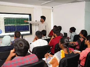
The demand for skilled VLSI professionals is growing rapidly, and RTL design and verification have become some of the most sought-after skills in the semiconductor industry. Our RTL Design Training in Pune is tailored to help fresh graduates and working professionals build a successful career in this field. With a structured curriculum and hands-on learning, our RTL Design Course in Pune equips learners with both the fundamentals and advanced concepts of RTL design and verification.
We are known for offering the Best RTL Design training with placement in Pune, where students receive not only in-depth technical knowledge but also dedicated placement support. As one of the most reliable RTL training institutes in Pune with 100% placement, we take pride in providing career-focused training that meets industry standards. Our RTL Design and Verification course in Pune covers every aspect of RTL coding, simulation, verification methodologies, and synthesis, ensuring students are job-ready from day one.
For those seeking advanced knowledge, the Advanced RTL design course Pune provides detailed insights into modern RTL design practices, verification techniques, and industry tool usage. At the same time, our Affordable RTL training courses in Pune ensure that high-quality training is accessible without financial strain.
To meet the needs of today’s learners, we offer flexible RTL design online and classroom training in Pune, so you can choose the mode that suits your schedule. Moreover, our RTL courses in Pune with job guarantee go beyond training by providing career guidance, interview preparation, and job placement opportunities.
Practical learning is a major part of our program. Through RTL design training with real-time projects Pune, students get the chance to work on industry-relevant projects that bridge the gap between theory and practice. This hands-on exposure builds confidence and prepares learners to face real-world design challenges effectively. Additionally, our RTL placement training in Pune includes resume building, mock interviews, and aptitude sessions to help students succeed during recruitment processes.
Upon completing the course, students earn an industry-recognized RTL certification course in Pune, which adds value to their resume and increases their employability in top semiconductor companies. For freshers, our dedicated RTL fresher jobs after training in Pune initiative provides the right support and guidance to help them secure their first role in the VLSI industry.
Our curriculum also includes RTL design flow training Pune, where learners understand the complete design flow—from specification and RTL coding to simulation and verification. This ensures a holistic understanding of the RTL design lifecycle, preparing students to handle complex projects with ease.
Enroll today in our RTL Design & Verification Training in Pune to gain advanced skills, real-time project exposure, and strong placement support. With expert mentors, affordable programs, and 100% placement assistance, we are committed to helping you achieve a rewarding career in VLSI design and verification.
"RTL Design Training in Pune , RTL Design Course in Pune , Best RTL Design training with placement in Pune, RTL training institutes in Pune with 100% placement, RTL Design and Verification course in Pune , Advanced RTL design course Pune , Affordable RTL training courses in Pune , RTL design online and classroom training in Pune, RTL courses in Pune with job guarantee, RTL design training with real-time projects pune , RTL placement training in Pune , RTL certification course in Pune , RTL fresher jobs after training in pune , RTL design flow training Pune "


Hours
Copyright 2025 © VLSI Technologies Private Limited
Designed and developed by KandraDigitalCopyright 2025 © VLSI Technologies Private Limited
Designed, Developed & Marketing by KandraDigital