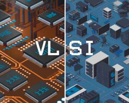
The semiconductor industry is evolving faster than ever, driving innovation in artificial intelligence, 5G, data centers, and autonomous systems. At the core of this revolution lies VLSI (Very Large-Scale Integration) — the process of designing and fabricating integrated circuits that power every modern electronic device.
Within the VLSI domain, physical design plays a crucial role. It bridges the gap between the logical (RTL) design and the actual silicon layout. To become a successful VLSI professional, mastering physical design tools is not just a skill — it’s a necessity. These tools automate complex design tasks, optimize performance, minimize power, and ensure that a chip meets timing, area, and power constraints before it goes to fabrication.
In this blog, we’ll explore the most important physical design tools every aspiring VLSI engineer should learn to build a strong career in the semiconductor industry.
What is Physical Design in VLSI?
Physical design refers to the stage of the VLSI design flow that deals with converting the logical or RTL design (written in Verilog or VHDL) into a geometrical representation that can be fabricated on silicon.
This process includes the following key steps:
- Design Setup and Initialization
- Floorplanning and Power Planning
- Placement of Cells and Macros
- Clock Tree Synthesis (CTS)
- Routing (Signal & Power)
- Physical Verification (DRC, LVS, ERC)
- Timing Closure and Signoff
Each of these stages requires specialized EDA (Electronic Design Automation) tools. Learning how to use them effectively is essential to excel as a physical design engineer.
Top Physical Design Tools Every VLSI Professional Must Learn
1. Cadence Innovus Implementation System
Cadence Innovus is one of the most widely used physical design tools in the industry. It enables end-to-end physical implementation, including placement, optimization, CTS, routing, and timing closure.
Why It’s Important:
- Industry standard for ASIC design
- Offers fast turnaround and power-performance optimization
- Integrates seamlessly with other Cadence tools like Tempus (timing) and Voltus (power analysis)
Key Features:
- High-performance placement and routing engine
- Multithreaded architecture for large designs
- Advanced power optimization techniques
- Signoff-level accuracy for timing and power
2. Synopsys IC Compiler II (ICC2)
Synopsys IC Compiler II (ICC2) is another top-tier physical design tool used across global semiconductor companies. It focuses on place and route (P&R) and enables engineers to implement highly complex designs efficiently.
Why It’s Important:
- Dominant in large-scale ASIC design environments
- Used for high-performance chips at 7nm, 5nm, and 3nm nodes
- Provides advanced optimization algorithms and tight integration with Synopsys Design Compiler and PrimeTime
Key Features:
- Ultra-fast P&R with high accuracy
- Machine learning-driven design optimizations
- Advanced timing closure techniques
- Excellent support for FinFET and GAA technologies
3. Mentor Graphics Calibre (by Siemens EDA)
Mentor Calibre is the industry-standard signoff tool for physical verification. After the layout is completed, Calibre checks the design for manufacturing readiness through DRC (Design Rule Check), LVS (Layout vs. Schematic), and ERC (Electrical Rule Check).
Why It’s Important:
- Ensures chip manufacturability and design rule compliance
- Required in every fabrication process (TSMC, Samsung, Intel, etc.)
- Used in every stage of signoff verification
Key Features:
- DRC/LVS/ERC signoff verification
- Reliability analysis and parasitic extraction
- Advanced node support down to 3nm
- Integration with both Cadence and Synopsys environments
4. Synopsys PrimeTime
While not a physical layout tool, PrimeTime is crucial for timing signoff and analysis in physical design. It verifies whether the design meets setup, hold, and path timing requirements across multiple process corners.
Why It’s Important:
- Industry-standard tool for STA (Static Timing Analysis)
- Helps achieve final timing closure before tape-out
- Integrated with Synopsys ICC2 for physical optimization
Key Features:
- Fast multi-corner, multi-mode analysis
- Signal integrity and OCV (On-Chip Variation) analysis
- Support for advanced process nodes
- Ansys RedHawk / Totem
Ansys RedHawk and Totem are used for power integrity and thermal analysis. These tools analyze IR drop, electromigration (EM), and thermal gradients that can affect chip reliability and performance.
Why It’s Important:
- Crucial for ensuring robust power delivery
- Mandatory for FinFET and 3D IC designs
- Used by foundries for signoff-level power verification
Key Features:
- Full-chip dynamic IR-drop analysis
- Electromigration and power grid verification
- Thermal-aware design analysis
6. Cadence Voltus
Voltus is Cadence’s power integrity and EM/IR analysis tool, often used alongside Innovus for signoff-level verification.
Why It’s Important:
- Offers dynamic power and voltage drop analysis
- Integrated seamlessly into the Cadence digital flow
Key Features:
- EM/IR signoff for advanced nodes
- Power grid optimization
- Thermal-aware design management
- Synopsys StarRC
StarRC is the leading tool for parasitic extraction, essential for accurate timing and power signoff. It extracts capacitance and resistance (RC values) from layout geometries.
Why It’s Important:
- Accurate RC extraction impacts final timing closure
- Foundry-certified signoff tool for advanced nodes
Key Features:
- Fast RC extraction for large designs
- Integration with PrimeTime and ICC2
- Multi-corner extraction for accuracy
Other Useful Tools to Learn
Apart from the top-tier tools above, here are other tools you should explore:
- Cadence Tempus: Timing signoff and ECO optimization
- Synopsys Fusion Compiler: Unified flow for synthesis and implementation
- OpenROAD / OpenLane: Open-source tools for learning ASIC flow
- Mentor AFS / Eldo: Analog and mixed-signal verification
How to Start Learning Physical Design Tools
- Learn the Basics of Digital Design – Understand logic gates, RTL coding, and synthesis.
- Study the Physical Design Flow – Get clear on placement, routing, and timing closure.
- Use Open-Source Tools – Start with OpenLane, Magic, or KLayout for hands-on practice.
- Get Familiar with Linux and TCL Scripting – Essential for automating design tasks.
- Join a VLSI Training Program or Internship – Hands-on experience is key.
- Practice Real Projects – Implement complete digital design flows and verify timing, area, and power.
Future Scope for Physical Design Engineers
With global investment in semiconductor manufacturing — including India’s Semiconductor Mission — demand for VLSI physical design engineers is at an all-time high. Mastery of tools like Cadence Innovus, Synopsys ICC2, PrimeTime, and Mentor Calibre will open doors to global semiconductor companies such as Intel, AMD, NVIDIA, Qualcomm, Samsung, Micron, and TSMC.
Future trends like chiplets, 3D ICs, GAAFETs, and AI-driven EDA will further expand opportunities for professionals skilled in advanced physical design flows.
Conclusion
Becoming a successful VLSI physical design professional requires more than theoretical knowledge — it demands hands-on experience with industry-standard tools. By mastering tools like Cadence Innovus, Synopsys ICC2, PrimeTime, Calibre, and RedHawk, you’ll gain the technical expertise needed to design and verify next-generation semiconductor chips.
As the semiconductor industry advances toward sub-3nm nodes, 3D architectures, and AI-driven design, physical design engineers will remain at the heart of innovation. Invest your time in learning these tools today — they’re your gateway to an exciting, high-demand VLSI career of the future.

Why Tool Familiarity Alone Is Not Enough in VLSI
Learn why knowing EDA tools alone is not enough for VLSI careers. Understand the importance of debugging, RTL coding, fundamentals, and problem-solving in semiconductor jobs.

What Industry Engineers Expect from Entry-Level VLSI Candidates
Learn what semiconductor industry engineers expect from entry-level VLSI candidates, including skills, projects, debugging, tools, and interview readiness.
_11zon.jpg)
How to Build Problem-Solving Skills for VLSI Interviews
Learn how to improve problem-solving skills for VLSI interviews through debugging, RTL practice, logic building, and real interview preparation strategies.

How Much Coding Is Enough for VLSI Verification Roles?
Learn how much coding is actually required for VLSI verification roles. Understand the importance of SystemVerilog, UVM, scripting, and practical debugging skills.

Math Required for VLSI – What You Need and What You Don’t
Worried about math in VLSI? Learn which mathematical concepts are actually required for VLSI careers and which topics are not essential for beginners.
.
Hours
Copyright 2025 © VLSI Technologies Private Limited
Designed and developed by KandraDigitalCopyright 2025 © VLSI Technologies Private Limited
Designed, Developed & Marketing by KandraDigital
