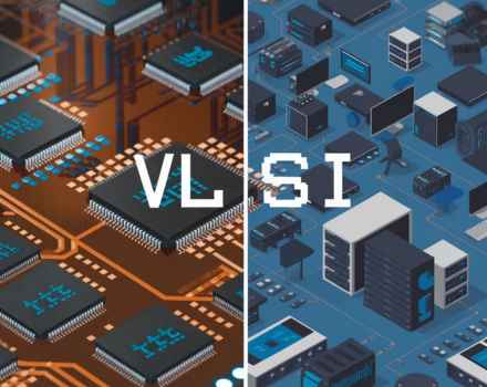
Physical Design and RTL Design are both critical stages in the VLSI (Very Large Scale Integration) design process, but they focus on different aspects of chip creation.
RTL Design (Register Transfer Level) is the first step in the design process. It involves defining the functionality of a chip using high-level abstractions. Designers describe the behavior of the system in terms of registers, data transfer, and operations using HDLs (Hardware Description Languages) like Verilog or VHDL. The main objective of RTL design is to ensure that the circuit behaves as expected in terms of logic and functionality. After completion, the design undergoes synthesis to convert it into a gate-level representation for the next phase.
Physical Design, on the other hand, comes after the RTL design is synthesized. It focuses on the actual implementation of the chip's logic on a silicon substrate. This stage involves tasks like placement, where components are positioned on the chip, and routing, where connections between components are made. The goal of physical design is to optimize the layout to meet performance requirements, such as timing, power consumption, and chip area, ensuring that the chip can be fabricated efficiently.
RTL Design vs Physical Design in VLSI
When comparing RTL vs Physical Design in VLSI, the primary distinction lies in the level of abstraction and the focus of each process. Let’s break this down
Abstraction Level
- RTL Design works at a high abstraction level, describing the logic of a circuit without considering its physical attributes.
- Physical Design, on the other hand, operates at a much lower level of abstraction, focusing on the physical layout of the circuit.
Design Focus
- RTL Design is more concerned with functionality and behavior, ensuring that the logic works as intended. It’s about defining how data flows through registers and how the various blocks interact.
- Physical Design is about ensuring that the logical design can be physically implemented and functions efficiently in terms of area, power, and timing.
Tools and Languages
- RTL Design uses HDLs like Verilog and VHDL to describe the functionality of the circuit.
- Physical Design uses EDA (Electronic Design Automation) tools like Cadence, Synopsys, and Mentor Graphics to handle tasks like placement, routing, and timing analysis.
Timing and Optimization
- RTL Design is concerned with ensuring that the logical design meets the required timing constraints in terms of clock cycles and signal propagation.
- Physical Design focuses on optimizing the timing at the physical level, considering factors like signal delay, wire length, and power consumption.
Final Goal
- RTL Design is about ensuring that the circuit works as per the design specifications and can be synthesized into a lower-level design.
- Physical Design is about making sure the circuit can actually be fabricated on a silicon chip and operates efficiently under real-world conditions.
RTL Design and Physical Design - Which One is Better?
The decision between RTL Design and Physical Design depends largely on personal interests, strengths, and career goals. Both areas offer distinct opportunities and challenges.
Career Growth: RTL Design is often considered the foundation of chip design, focusing on the logical and functional aspects to ensure a chip behaves as intended. Physical Design, on the other hand, requires a deep understanding of gate-level circuits and optimization to address real-world challenges like power consumption and signal integrity.
Skill Set: RTL Design demands proficiency in HDLs like Verilog and VHDL and a strong grasp of digital logic. Physical Design, however, requires knowledge of semiconductor physics, EDA tools, and timing analysis, as well as an understanding of physical constraints in chip design.
Demand Both fields are in high demand, particularly as semiconductor manufacturing advances. RTL Design is essential for companies focused on functional verification, while Physical Design plays a critical role in chip optimization and manufacturing.
RTL and Physical Design Salary Comparison
When choosing between RTL Design vs Physical Design, one of the key factors that often influences career decisions is the salary. Both roles offer competitive compensation, but there are notable differences in the salary structures for each. Let’s dive into the RTL and Physical Design Salary Comparison to understand how earnings differ based on experience, skills, and industry demand.
In India, both RTL Design and Physical Design professionals can expect lucrative salaries. Entry-level positions in RTL Design generally offer a salary range of ₹6,00,000 to ₹8,00,000 annually, whereas Physical Design engineers may start at slightly higher figures, with salaries typically ranging from ₹7,00,000 to ₹9,00,000 per year. This initial salary gap can be attributed to the specialized skills required for physical design, which often involves intricate work with physical chip layouts and optimizations.
As professionals gain experience, the salary gap between the two roles becomes more pronounced. Mid-career engineers in RTL Design can earn between ₹9,00,000 to ₹12,00,000, while those in Physical Design can expect salaries in the range of ₹11,00,000 to ₹14,00,000. This difference reflects the higher demand for Physical Design skills, especially as companies focus on improving the performance and manufacturability of semiconductor chips.
For senior-level professionals, the salary potential in both fields can be substantial. Senior RTL Design engineers with years of experience can command salaries upwards of ₹15,00,000 annually. However, Physical Design experts—due to their expertise in optimizing the physical aspects of the chip—can often earn even higher figures, with salaries reaching ₹16,00,000 or more.
While both RTL and Physical Design Salary Comparison shows that both career paths offer strong earning potential, Physical Design professionals tend to have a slight edge in terms of salary due to the specialized and critical nature of their work. However, individual compensation will still depend on factors like location, company size, and expertise in specific tools and technologies.
Conclusion
The decision between RTL Design vs Physical Design ultimately boils down to your interests and career goals. RTL Design allows you to work on the functional and logical aspects of circuit design, which is crucial for the initial stages of chip development. Physical Design, on the other hand, focuses on the layout, optimization, and realization of the chip’s design in the physical world, often requiring more detailed technical expertise.
Both fields are vital in the VLSI design process, and there is no clear “better” option, as each offers unique challenges and rewards. Whether you choose RTL or Physical Design, both are integral to the world of semiconductor design and present promising career opportunities with competitive salaries. The key is to find the area that aligns with your strengths and interests to build a successful career in this dynamic and ever-evolving field of VLSI technology.

Why Tool Familiarity Alone Is Not Enough in VLSI
Learn why knowing EDA tools alone is not enough for VLSI careers. Understand the importance of debugging, RTL coding, fundamentals, and problem-solving in semiconductor jobs.

What Industry Engineers Expect from Entry-Level VLSI Candidates
Learn what semiconductor industry engineers expect from entry-level VLSI candidates, including skills, projects, debugging, tools, and interview readiness.
_11zon.jpg)
How to Build Problem-Solving Skills for VLSI Interviews
Learn how to improve problem-solving skills for VLSI interviews through debugging, RTL practice, logic building, and real interview preparation strategies.

How Much Coding Is Enough for VLSI Verification Roles?
Learn how much coding is actually required for VLSI verification roles. Understand the importance of SystemVerilog, UVM, scripting, and practical debugging skills.

Math Required for VLSI – What You Need and What You Don’t
Worried about math in VLSI? Learn which mathematical concepts are actually required for VLSI careers and which topics are not essential for beginners.
.
Hours
Copyright 2025 © VLSI Technologies Private Limited
Designed and developed by KandraDigitalCopyright 2025 © VLSI Technologies Private Limited
Designed, Developed & Marketing by KandraDigital
