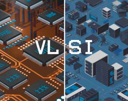
Introduction:
In the dynamic world of
semiconductor design, understanding the distinction between VLSI Front End and
Back End roles is essential for aspiring engineers and seasoned professionals
alike. The Front End encompasses the initial stages of chip design, focusing on
conceptualization, architecture development, and RTL coding. In contrast, the
Back End involves the physical implementation of the design, including tasks
like floor planning, placement, and routing.
By delving into the nuances of VLSI Front End vs Back End,
individuals gain insight into diverse career pathways within the semiconductor
industry. This introduction sets the stage for exploring the myriad
opportunities, job roles, and salary differentials that characterize these two
domains, particularly within the context of the Indian semiconductor landscape.
Stay tuned as we unravel the intricacies of VLSI Front End vs Back End,
providing valuable insights for those navigating their career journey in semiconductor
design.
What is Front End and Back End in VLSI?
In the landscape of Very Large Scale Integration
(VLSI) design, understanding the distinction between Front End and Back End
processes is fundamental. What is Front End and Back End in VLSI?
The Front End of VLSI
design encompasses the initial stages of chip development. Engineers in this
phase focus on conceptualizing the architecture, designing the logic, and
coding at the Register Transfer Level
(RTL). They employ hardware
description languages like Verilog and VHDL to create functional models of the
digital circuits. Additionally, Front End engineers engage in tasks such as
simulation, synthesis, and functional verification to ensure the correctness
and functionality of the design before proceeding to physical implementation.
Conversely, the Back End
of VLSI design deals with the physical realization of the chip. This phase
involves translating the logical design from the Front End into a physical
layout that can be manufactured. Back End engineers focus on activities such as
floor planning, placement and routing, timing closure, and design for
manufacturability (DFM). Their goal is to optimize the chip layout for
performance, power, and area while addressing manufacturing constraints.
In summary, while the
Front End primarily deals with the logical and functional aspects of chip
design, the Back End focuses on the physical implementation and layout. Both
phases are integral to the VLSI design process, working collaboratively to
bring innovative semiconductor products to fruition.
Understanding the roles
and responsibilities within each phase is crucial for aspiring VLSI engineers,
as it enables them to specialize in areas that align with their interests and
career goals. Moreover, recognizing the distinction between Front End and Back
End roles is essential for navigating the diverse opportunities and career
paths available in the semiconductor industry.
Opportunities and Job Roles:
In the domain of Very
Large Scale Integration (VLSI), understanding the distinction between what
is front end and back end in VLSI is crucial for aspiring engineers. The
front end involves the initial stages of chip design, encompassing conceptualization,
architecture development, and RTL (Register Transfer Level) coding. On the
other hand, the back end focuses on physical implementation, including floor
planning, placement, routing, and design for manufacturing (DFM).
Opportunities and job
roles within these domains vary significantly. Front End engineers are
responsible for RTL coding, synthesis, and functional verification, while Back
End engineers specialize in physical design optimization and ensuring the
manufacturability of the chip.
Understanding these
distinctions is essential for individuals looking to pursue a career in VLSI,
as it enables them to align their skills and interests with the diverse
opportunities available in both Front End and Back End roles.
- Front End Opportunities:
- Front End Design Engineers:
Responsible for RTL coding, synthesis, and functional verification of
digital logic.
- Verification Engineers:
Specialize in verifying the correctness of the design through simulation,
formal verification, and emulation techniques.
- Design
Automation Engineers: Develop tools and
methodologies to streamline the Front End design process and improve
productivity.
- Back End Opportunities:
- Physical Design Engineers: Focus
on floor planning, placement, and routing to achieve optimal chip layout
and performance.
- Timing Closure Engineers:
Ensure that the design meets timing requirements by analyzing and
addressing timing violations.
- DFM
Engineers: Address manufacturing-related
issues such as lithography, mask design, and process variability to
enhance chip yield and reliability.
VLSI Front End vs. Back End Salary in India:
In the realm of VLSI design in India,
understanding the salary differentials between Front End and Back End roles is
crucial for professionals seeking to navigate the semiconductor industry's job
market.
Front End Salary: Front End roles, encompassing tasks such as RTL
coding, verification, and design automation, often command higher salaries
compared to Back End positions. Experienced Front End engineers with expertise
in RTL design and verification methodologies can expect lucrative compensation
packages. The average annual salary for VLSI Front End engineers in India
ranges from(1 year experience) ₹4 lakhs to ₹6 lakhs, depending on factors such
as experience level, skill set, and geographical location.
Source:https://www.ambitionbox.com/profile/vlsi-verification-engineer-salary?experience=3
Back End Salary: While Back End roles involving physical design,
timing closure, and design for manufacturing are equally essential in the chip
development process, Back End engineers, responsible for tasks like floor
planning and routing, may earn between (1 year experience) ₹5 lakhs to ₹7 lakhs
per annum in India. However, specialized roles in physical design optimization
or timing closure may offer higher compensation packages.
Source:https://www.ambitionbox.com/profile/vlsi-physical-design-engineer-salary
Considerations: Considering VLSI Front End vs Back End salary
roles can vary based on factors such as experience, expertise, location, and
the specific demands of the role. Companies in technology hubs like Bangalore,
Hyderabad, and Pune often offer competitive salaries to attract top talent in
the semiconductor industry. Additionally, professionals with advanced degrees,
certifications, or specialized skills may command higher salaries irrespective
of the Front End or Back End designation.
Conclusion:
In conclusion, the
comparison between VLSI Front End and Back End roles provides valuable insights
into the dynamic landscape of semiconductor design, particularly in India.
While both domains offer rewarding opportunities, it's evident that there are
subtle yet significant differences in salary and job roles.
Professionals venturing
into the Front End arena often find themselves at the forefront of innovation,
focusing on logical design, RTL coding, and functional verification. With
higher demand for skilled RTL designers and verification engineers, salary
packages in this domain tend to be slightly more lucrative.
On the other hand, Back
End engineers play a critical role in translating logical designs into physical
layouts, ensuring optimal chip performance and manufacturability. While salary
packages for Back End roles may be slightly lower compared to Front End
positions, opportunities for specialization and growth abound.
In the Indian
semiconductor industry, the VLSI Front End vs Back End salary reflect
the demand-supply dynamics and the specialized skill sets required in each
domain. However, it's essential to note that career satisfaction and growth
potential are equally important considerations for professionals navigating
their paths in VLSI design.
Ultimately, whether one
chooses to embark on a journey in VLSI Front End or Back End, the industry
promises ample opportunities for learning, growth, and innovation, shaping the
future of semiconductor technology in India and beyond.

Why Tool Familiarity Alone Is Not Enough in VLSI
Learn why knowing EDA tools alone is not enough for VLSI careers. Understand the importance of debugging, RTL coding, fundamentals, and problem-solving in semiconductor jobs.

What Industry Engineers Expect from Entry-Level VLSI Candidates
Learn what semiconductor industry engineers expect from entry-level VLSI candidates, including skills, projects, debugging, tools, and interview readiness.
_11zon.jpg)
How to Build Problem-Solving Skills for VLSI Interviews
Learn how to improve problem-solving skills for VLSI interviews through debugging, RTL practice, logic building, and real interview preparation strategies.

How Much Coding Is Enough for VLSI Verification Roles?
Learn how much coding is actually required for VLSI verification roles. Understand the importance of SystemVerilog, UVM, scripting, and practical debugging skills.

Math Required for VLSI – What You Need and What You Don’t
Worried about math in VLSI? Learn which mathematical concepts are actually required for VLSI careers and which topics are not essential for beginners.
.
Hours
Copyright 2025 © VLSI Technologies Private Limited
Designed and developed by KandraDigitalCopyright 2025 © VLSI Technologies Private Limited
Designed, Developed & Marketing by KandraDigital
